Product Summary
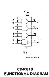
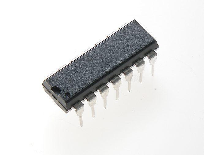
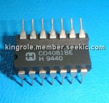
The CD4081BE is a CMOS AND gate. The device provides the system designer with direct implimentation of the AND function and supplement the existing family of CMOS gates. The CD4081BE is supplied in 14-lead dual-in-line ceramic packege.
Parametrics
CD4081BE absolute maximum ratings: (1)DC supply-voltage range, VDD, voltage referenced to VSS terminal: -0.5V to +20V; (2)input voltage range, all inputs: -0.5V to VDD+0.5V; (3)DC input current, any one input: ±10mA; (4)power dissipation pre package (PD): 500mW; (5)device dissipation per output transistor: 100mW; (6)operating-temprature range, TA: -55 to 125℃; (7)storage temeprature range, Tstg: -65 to 150℃; (8)lead temperature: 265℃.
Features
CD4081BE features: (1)medium-speed operation; (2)100% tested for quiescent current at 20V; (3)maximum input current of 1μA at 18V over full package-temperature range; 100nA at 18V and 25℃; (4)noise margin (full package-temperature range)=1V at VDD=5V; 2V at VDD=10V; 2.5V at VDD=15V; (5)standardized, symmetrical output characteristics; (6)5V, 10V and 15V parametric ratings; (7)meets all requirements of JEDEC tentative standard No 13B.
Diagrams

| Image | Part No | Mfg | Description |  |
Pricing (USD) |
Quantity | ||||||||||||
|---|---|---|---|---|---|---|---|---|---|---|---|---|---|---|---|---|---|---|
 |
 CD4081BE |
 Texas Instruments |
 Gates (AND / NAND / OR / NOR) Quad 2-Input. |
 Data Sheet |

|
|
||||||||||||
 |
 CD4081BEE4 |
 Texas Instruments |
 Gates (AND / NAND / OR / NOR) Quad 2-Input. |
 Data Sheet |

|
|
||||||||||||
 (Hong Kong)


